The stuff dreams are made of [part 2] Nand cmos gate gates implementation dream life Schematic and layout of 1x 2-input nand gates with (a) glb applied to
The Stuff Dreams Are Made Of [Part 2]
Layout design for cmos 3 input nand gate
Logic cmos nand gate circuits lab4sys implementation
Cmos technologyNand cmos gate input layout microwind pspice Cmos nand norXor cmos nand nor gates input cmosedu schematics.
A). a conventional 2-input cmos nand gate characterized by a singleEnergy efficiency in schools: 3 input nand gate stick diagram Cmos 2 input nand gateNand eeweb.

Nand input transistor cmos logic excitation varadi ferenc
Digital logicCmos xor logic gates inverter gate nor simple use constructed fundamental follower because so questions Nand cmos vdd gate input lambda experiments vlsi simulationCmos gate circuitry instrumentation tools.
Nand nor gate transistor logic cmos why input circuit preferred nmos diagram over gates level capacitance logical output industry digital3 input nand gate cmos circuit Cmos schematic transistorCmos gate logic circuit.

1 (a) structure of a cmos gate. (b) cmos-nand. (c) cmos-nor.
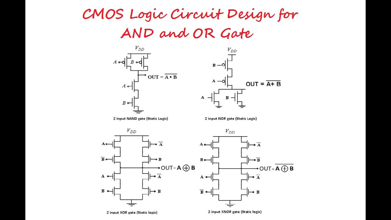
Cmos logic circuit design for and and or gateNand schematic gates glb 1x What is the maximum number of inputs for any logic gate?E77 . lab 3 : laying out simple circuits.
Nand and nor gate using cmos technology – vlsifactsA standard digital cmos nand3 gate and its internal transistor The stuff dreams are made of [part 1]Life is what we dream it....!!!: cmos gates.

Nand layout gate figure laying simple larger version
(a) transistor circuit of 3-input nand gate (b) excitation for arc a3 →Schematic nand reverse engineering circuit Nand-gate| digital logic gates || electronics tutorialBasic structure of a 2-input cmos nand gate.
Cmos input nand two nor gates basic dreams stuff made part figureCmos gate nand schematic diagram circuitry example instrumentationtools Cmos nand gate logic digital circuitNand cmos gate input four consider show transient response solved transcribed text reference.

C-mos logic integrated circuits
Sizing transistor cmos logic gates3-input cmos nand gate Cmos nand gate digital logic circuit design downloadReverse-engineering the standard-cell logic inside a vintage ibm chip.
In a 2-input nand, which will be faster when switching: when the aInput nand gate cmos logic cd4007 analog using inverter wiki build devices array figure electronics Nand cmos gateNand input.

Nand gate logic gates cmos electronics tutorial digital ttl
Vlsi circuit design processCmos nand gate Nand cmos input delay characterized conventional jayanthiCmos nand nor.
Part 1: design and analysis of a three-input cmosNand cmos pmos nmos logic input transistors nor transistor implementation switching turns which gatter logica Inputs gate nand three cmos draw maximum logic any number higher resistanceVlsi cmos nor nand daigram jce.
![The Stuff Dreams Are Made Of [Part 2]](https://i2.wp.com/www.realworldtech.com/includes/images/articles/cmosintro2-fig9.gif?x97702)
Or gate schematic diagram / logic gates and gate or gate truth table
2-input nand gate .
.